
The Coming Age Of 3D Integrated Circuits
The pedagogical model of the integrated circuit goes something like this: take a silicone wafer, etch out a few wells, dope some of the silicon with phosphorous, mask some of the chip off, dope some more silicon with boron, and lay down some metal in between everything. That’s an extraordinarily basic model of how the modern semiconductor plant works, but it’s not terribly inaccurate. The conclusion anyone would make after learning this is that chips are inherently three-dimensional devices. But the layers are exceedingly small, and the overall thickness of the active layers of a chip are thinner than a human hair. A bit of study and thought and you’ll realize the structure of an integrated circuit really isn’t in three dimensions.
Recently, rumors and educated guesses coming from silicon insiders have pointed towards true three-dimensional chips as the future of the industry. These chips aren’t a few layers thick like the example above. Instead of just a few dozen layers, 100 or more layers of transistors will be crammed into a single piece of silicon. The reasons for this transition range from shortening the distance signals must travel, reducing resistance (and therefore heat), and optimizing performance and power in a single design.
The ideas that are influencing the current generation of three-dimensional chips aren’t new; these concepts have been around since the beginnings of the semiconductor industry. What is new is how these devices will eventually make it to market, the challenges currently being faced at Intel and other semiconductor companies, and what it will mean for a generation of chips several years down the road.
The History of 3D Chips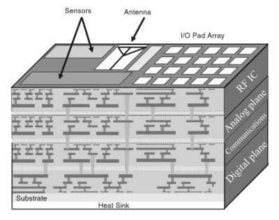 Many different circuits on the same die, tied together with three-dimensional interconnects. Image source: Pavlidis & Friedman, Three-dimensional Integrated Circuit Design (2010)
In the late 1960s and early 1970s, chips became increasingly complex. The forefront of semiconductor technology moved from op-amps and small digital packages to semiconductors with thousands of transistors, and with this came in increasing reliance on interconnects between different portions of these chips.
In the march of technology over the past fifty years, transistors have gone from something you can see with the human eye to tiny specks only a few atoms wide. Interconnects become the dominant design choice, especially with ever-increasing complexity of designs, increasing bus width, and more numerous inputs and outputs.
Because all but the most basic integrated circuits are inherently three-dimensional, the obvious choice for where to put these interconnects was the same solution in any sprawling metropolis; if you can’t grow out, grow up.
This line of research continued throughout the 1970s, 1980s, and 1990s as an academic pursuit, with solutions to new problems. How do you cool the inside of a cube? You can put cooling channels throughout the entire chip. While these problems were simple to define, and the solutions easy to explain, taking the entire idea through manufacturing to a finished product was hard. A much easier way to increase transistor density was to stack individual packages on top of each other.
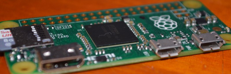 The main chip on the Raspberry Pi Zero is actually two ICs. The bottom is the ARM processor, while the top is the DRAM. This is known as a Package on Package (POP) assembly.
These Package on Package devices can be seen – albeit at an oblique angle – on dozens of devices. The large chip on the Raspberry Pi Zero, Model A, and Model B are POP devices, with the RAM on the top chip connected directly to the Broadcom CPU. The latest, highest capacity RAM modules also use this technique. The JEDEC standards for memory don’t account for 16GB DDR3 modules, but that doesn’t mean you can’t buy them. Here, again, PoP devices are how companies are getting around the problems of interconnects.
The Current State of 3D Chips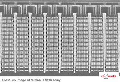 Samsung’s V-NAND [image source] While the idea of 3D chips constructed out of multiple layers of silicon is an old idea, only recently have we seen this sort of technology make it into consumer devices. In 2013, Samsung moved into the 3D Flash market with V-NAND, regarded as the first true production-grade 3D transistor technology.
Chipworks did a terrific teardown of Samsung’s V-NAND found in Samsung’s 850 Pro SSDs. It is, by any measure, an incredible feat of engineering. The V-NAND stack found in these SSDs are a 38-layer sandwich of transistors, with each transistor holding one bit of information.
This innovation obviously allows Samsung to put more transistors into a small area, leading to higher capacities. If you believe the Samsung marketing material, up to 100 layers of transistors can be stuffed onto a chip, paving the way for very, very high-capacity drives. This capacity isn’t the only benefit; thanks to the construction of V-NAND, interference between memory cells is reduced, making the drive more power efficient. Write endurance – the number of times a memory cell can be written to without going bad – is improved over normal 2D NAND Flash.
 Even if most of the claims about Samsung’s V-NAND 3D Flash technology are marketing wank, you can’t deny it’s a very good SSD. Look on any ‘build suggestion’ thread in the forums of any PC-based community, and you’ll find a Samsung 850 Pro SSD somewhere in the parts list. 3D Flash is a technological triumph and a market success. The question on everyone’s mind then becomes ‘when is it going to be more than just SSDs?’
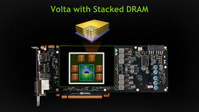
The next generation of Nvidia GPUs, Volta, will feature stacked DRAM when it is released in 2018. While this is about the same level of complexity as stacked NAND Flash, it does tell us that 3D chips are hitting the mainstream, and it’s only a matter of time before we can think of a CPU as a true 3D device, and not just a few layers placed on top of each other.
3D CPUsIf you trace the origins of interesting technological achievements in semiconductors, the usual progression begins with universities, moves into production with memories, and finally becomes part of the glue that holds CPUs together. At one time, Intel was best known for their very high-capacity DRAM chips (hundreds of bytes!), before the knowledge gained in their manufacture moved over to CPUs.
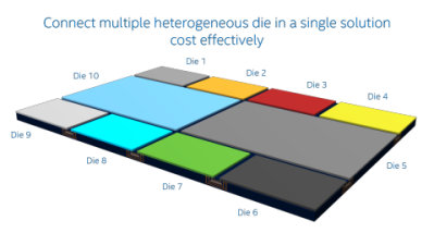 Intel’s EMIB. [image source] This inevitably means CPUs designed with dozens of layers. For Intel, the next big advancement is the Embedded Multi-die Interconnect Bridge (EMIB), that takes the PoP concept, strips it of epoxy, and does everything at a much lower level. The EMIB is effectively a backplane between dies. By putting multiple dies on a single piece of silicon, with vias tunneling in a zigzag fashion, Intel can put many different circuits on a single piece of silicon.
While putting multiple dies on a single piece of silicon will be a boon for Intel – especially with the Altera IP in their portfolio – it’s not exactly a true three-dimensional chip. That will have to wait a while; we’ve only had 3D Flash for a few years now, and 3D RAM won’t be public for another two years. Making a 3D CPU is a much more complex engineering challenge, and for that we may be waiting the better part of a decade.
Three dimensional chips will be released, though. It’s only a matter of time. There’s simply no other way to increase the density of interconnects, the number of devices on a chip, or speed than by moving into a third dimension of silicon.
0 comments:
Post a Comment